I found some boards being sold as scrap. Harvest the gold......
The gold I see is the old components that are not being made any longer. A little research lead me to believe they are the first junction transistors made by TI. The story line goes like this. TI bought a license and the machine to make them from IBM. TI produced them for IBM. The numbers should have a date and component ID in them. In that day they even gave each device a serial number (some not all). So I make a giant leap and say it is an IBM device made by TI and excess IBM couldn't use was sold to GE. So what's in that TO5 can?
WOW! It took good eyes to set them up to be soldered? Maybe the machine did it??
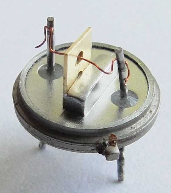
A little more detail. The die is mounted over a hole in the base plate and the wire passes thru the hole to be soldered on.
The can is the base and the leads are emitter and collector.
I removed the top on a couple I had in the parts bin to see how they compare to the IBM.
My pictures are not as good as theirs. They probably used a real camera. I'm using a cell phone. They do appear to be made using the same design.
* The ones I disassembled are Russia 39B PNP.
** The boards arrived. I found four transistors with different marking. They all tested good. They were all PNP types with different ß and forward voltage. The Transistor Museum had an article showing some like mine and noted they have different colored epoxy filler. They questioned if the color was a code, maybe type ID? I tested some green and black ones. They were all PNP but did have different ß and forward voltage. If there is a code I failed to see it.


No comments:
Post a Comment