
Friday, March 15, 2019

Monday, March 11, 2019
What's it - part 2

The gold I see is the old components that are not being made any longer. A little research lead me to believe they are the first junction transistors made by TI. The story line goes like this. TI bought a license and the machine to make them from IBM. TI produced them for IBM. The numbers should have a date and component ID in them. In that day they even gave each device a serial number (some not all). So I make a giant leap and say it is an IBM device made by TI and excess IBM couldn't use was sold to GE. So what's in that TO5 can?


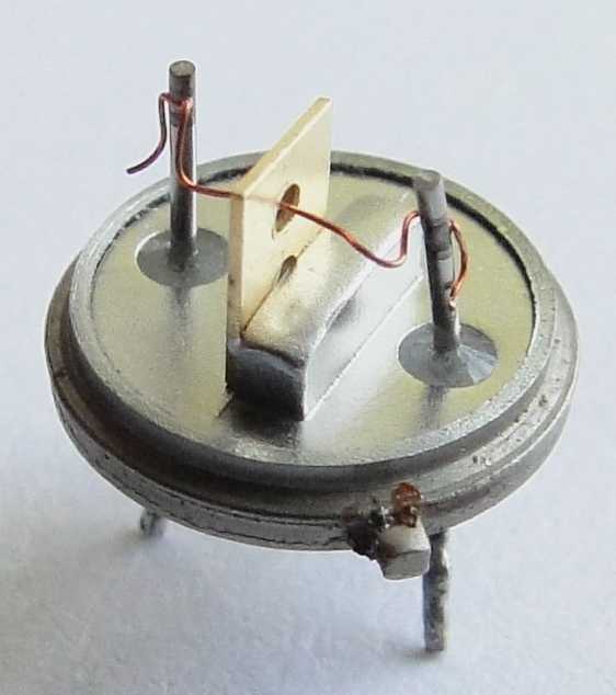
I removed the top on a couple I had in the parts bin to see how they compare to the IBM.


* The ones I disassembled are Russia 39B PNP.
** The boards arrived. I found four transistors with different marking. They all tested good. They were all PNP types with different ß and forward voltage. The Transistor Museum had an article showing some like mine and noted they have different colored epoxy filler. They questioned if the color was a code, maybe type ID? I tested some green and black ones. They were all PNP but did have different ß and forward voltage. If there is a code I failed to see it.
Friday, March 8, 2019
What's It?

It's a 1960s circuit board.
Probably IBM (patent) transistors, made by TI for GE.
Thursday, March 7, 2019
Plate Bend or Square Law detection.

Tuesday, March 5, 2019
Voltage gain Vs Power Gain
You can use the amp for headphone or earbud. I designed it for my earbud. I buy them at dollar tree for a $1 each. They have headphones too, I like the ear bud better. Any way I ran the sim for both so you can see how that works.
 With my earbud I get 175mv-pk.
 With the headphone I get over 400 mv-pk. So which is better? The one you have of course. Oh well if you have a choice which would perform better with this amp?
 Wow 75 uw should drive the headphone well. Actually 1 or 2 uw will drive a sound powered phone well.
 But look at the ear bud. Close to 500 uw. Yes the ear bud will produce as much sound as the headphone. The earbuds are rated 90dbm - 110dbm and the phone is rated up to 120dbm. The phone is a little more sensitive but the amp will drive the earbud harder with a smaller input.
I have been using this amp to drive a single earbud. The plug was bad on the bud so I split the cord and made 2 singles. The little amp drives the single bud very well.


I have been using this amp to drive a single earbud. The plug was bad on the bud so I split the cord and made 2 singles. The little amp drives the single bud very well.
Wednesday, February 27, 2019
AF Amp with gain control


Sunday, February 24, 2019
AF Amp circuit operation

Q3 is a phase splitter.
Q1 and Q2 are a push-push amplifier.
* connecting a center tapped transformer in the output circuit would produce a push-pull amplifier. This is how I was taught 50 years ago. Today the terminology may have changed?
Anyway the key is Q1 and Q2 bases are being driven out of phase. Q1 and Q2 operating class B (conducting 50% of the time) feed the load a full cycle with one transistor biased off while the other conducts. (or AB with one being throttled down while the other is driven harder.)

When Q1 is driven into conduction current flows from C1 DOWN thru Q1 to ground and UP from ground thru R3. Discharging C1.


It is a good earbud driver as I made mine but you can adjust the bias and add more power as desired.
Good luck!
Subscribe to:
Posts (Atom)