Saturday, December 29, 2018

transistor action examined in spice sim

It seems the transistor and the vacuum tube share a lot of characteristics. The vacuum tube current is limited by the amount of electrons the filament or cathode can emit. Applying more plate voltage can not cause the heater or cathode to be able to emit more electrons. At very low plate voltage the space charge building around the cathode can make it harder for the emission to occur. Once the plate voltage is high enough to draw them away the current limit will be the cathode ability. It is much the same with the transistor. The emitter injects carriers into the base. (the carriers could be electrons or holes for this discussion we will assume electrons.) The collector draws the carriers from the base. The crystal structure will only support a finite number of carriers. If the collector fails to remove them the base will become saturated or loaded with them. In transitor datasheets we find the ß listed or hfe. This is the relative ability of the collector to draw the carriers away in relation to the number drawn to the base. Let's look at some pictures and see if they make this clearer.
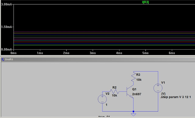
 I applied 1 volt to the base through a 10K resistor.  This sets the base current used in the test. I am stepping the collector from 3 to 12 volts in 1 volt steps. As you can see the collector current is very close to steady state.( we'll look at the reason for the small change later.)

I expanded the scale to show the variation.The collector resistor is increased to 10K. The current is varying. Why?
The voltage Vce is at saturation. In other word the 10K resistor is limiting the collector current and the base is filling up with carriers that cannot be drawn away. To put it another way. The voltage drop across the 10K resistor would have to exceed the supply voltage for more current to flow. The transistor resistance and the 10K resistor form a voltage divider. The semiconductor resistance varies with the current flowing in the circuit.
With a 1K resistor for the load the transistor can supply the current and the voltage drop across it is close to the applied. Again the emitter inject a set number of carriers with the applied bias and the collector draws them away. The drop across the 1K resistor remains the same so the collector voltage increases as the supply increases.
With a 1 ohm resistor we see basically the same step with supply change. As I said before the collector potential draws away carriers until the out flow equals the emitter injection and then the circuit is at equilibrium. Vce is equal Vcc - Vr3.
 This is what happens when we change the current through the base. Stepping E from 1 to 10 in 1 volt steps. Look closely and you can see the family of lines. E steps to a point and V1 steps through its values and E steps to the next point. Ic varies slightly as V1 swing threw its range.
Here we have Vcc = 100 volts as we swing the base bias. The higher Vcc will allow higher currents but the transistor can still be cutoff or biased on.
Here we see the relation between the base voltage and the collector current with Vcc = 100 volts.
Cutting the Vcc in half doesn't have that much effect on Ic.
Cutting Vcc back to 12 volts still give 2.45ma. Notice the base emitter voltage is swing slightly. The transistor has a resistance which varies with applied potential. With higher voltage drawing the carriers away at a faster rate the opposition to more being injected is less and as higher currents flow the voltage drop increases. So the final change is determined by the material resistance and the injection opposition. Doping heavy increases the ability to inject and reduces the resistance but there is more to it than that.
The problem with computer volt meters can be resolution. While we benefit from the wiggly lines we can also see more than a simple volt meter will display. Here I set the range to show the base voltage swing with a Vcc from 10 to 100 volts.
The change is still there but as I said before it is steady for practical purposes. Rbe in series with the 10K resistor form a voltage divider that drops the Vbe. Generally the 10K is large enough that changes in Rbe can be ignored. That effect is showing up in my sims. I guess that would be the topic another day.

in summary.
TRANSfer of reSISTance or transistor as we say.
Low resistance emitter to high resistance collector circuit.
inject carrier into the emitter and let the collector resistance fall. We could use Fermi level, barriers etc. but the sims tell the story quite well???

Thursday, December 27, 2018

Reversing a transistor hookup - will it work

A subject that comes up now and then is "can the circuit work as connected?" The circuit will likely be a Germanium transistor and then the discussion goes kind of mystic and implies the transistors are just beyond understanding. Oddly the board expert will throw out terms like Ebers-Moll.  Then we hear it is a Germanium being leaky and some other rubbish. So is it possible the circuits work are do we we have a few hundred circuits presented in the old books and magazines that just were untested and will not work?
Oddly when the Ebers-Moll enters the discussion it is with no explanation and is just to impress the readers so let us look at the model.

Ebers-Moll sees the transistor as 2 diodes connected back to back. One is forward biased and one is reversed biased. Would this model represent a real world transistor? Let us look at a couple of them.
This example is 2 diodes sharing the base connection. They are made with the same doping so would be represented by the model quite well. (the exception being the common connection rather than 2 cathodes.) This would be an early transistor such as found in the old books.
A later transistor is the epitaxial shown here. This time we see n- , n+ and p-. What they tell us is the doping levels are not the same. + is heavy doping while - is lightly doped. The 2N2222 is a planar epitaxial transistor so I will use it for the test. (The 2N2222 is the negistor I used in my simple oscillator.)
A quick look at this circuit will reveal I have installed it upside down yet with 10mv in I get 600mv out. A gain of 60 with a backward connected circuit!
I rotated the transistor to the 'proper' position and now have a loss in signal.
I adjusted the bias and now have the gain of 60 with the transistor installed properly. Why did I need to adjust the bias? Remember the p+ and n-? The doping is so a small base emitter current can control a larger emitter collector current. The heavily doped emitter injects carriers more efficiently.

Some food for thought,eh?

EDIT: I should point out the power handling ability of the transistor will need to be watched if using the circuit. The question would be ,'what is the base current?' Using a higher base current could burn the base out. It might be worth a test board.
EDIT 2: I think a 2N5550 will work backwards too.
Another circuit to test.

Wednesday, December 12, 2018

amp with voltage feedback and constance current?

The last amp was minimalistic this one has more components. Let's look at the sim.
It looks pretty good but I want to reduce low frequency response to reduce noise.
Reducing the capacitor values produces low frequency rejection.
I reduced the caps more and the low end lifted higher. In my build I used 56 pfd caps and the cutoff is about 200 Khz.
This is the final build except the C1 and C2 are 56 pfd. I did a little testing and found it to be more stable and noise free than previous designs. It should work with any general purpose transistor. The sim ran with the 2N2222 and 2N3904 gave a higher gain than the KSP10.
I put this one in a metal box. Maybe tomorrow  I can make a couple of pictures.
NOTE: I added the 4 ohm resistor in the emitter circuit to give a little more feedback and provide stability. It could work as well without it. The amp I made last week could have benefited from that addition.

Tuesday, December 11, 2018

LC Filter with Motorola AN on filter design

AN267
This app note was used to develop the program used to make the following screen shot data.

The cap goes from input to ground and the coil is in series with the head phones. I assumed 2K phones for the sim.
This is the frequency response. As frequency increases the coil rejects and the cap passes the signal.


Sunday, December 9, 2018

Lady Bird Radio or how to layout a breadboard

How would you go about laying out a board such as this?

My method may not be the best but it doesn't require any special software. I load the schematic in the graphics editor (paint). Go through the schematic and number the tie points. Layout the board with two or three rows of pins and number the pins so the components will connect between them.

I did not do this one it came from the web. It is for the board in the first picture.This method is presented in the book "Making a Transistor Radio". His board used screws and finish washers.

Making a Transistor Radio

By G C Dobbs

Saturday, December 8, 2018

When to Z match or how the match effects the source

When Z gen = Z load efficiency is 50%. Half of the power is lost in the generator. Consider the effect this would have on the generator feeding power to your home. When Zgen is zero efficiency is 100%. If I made a 100 watt audio amp would I want my transistors dissipating 50 watts? Food for thought.

Friday, December 7, 2018

Final build of the two stage amp - some observation

This project shows some of the interaction between stages and some design considerations. In any new design we must give and take, make a high gain circuit and have more noise and instability or reduce the gain and be stable with less noise. The final question is 'how much gain is enough?'. Where to put the gain is a good question also. I was throwing out such questions on another project and said the components are only a nickle each so use as many as seems useful. My friend and advisor on the project sent me this.
What do you think he was telling me?

Anyway I built the circuit and it was to strong. With the antenna lead about 1" from the amp input I received a station on 1160KHz. It was the USA Old Time Radio Network broadcasting with 5KW night time power Dallas Texas. The map program says 552 miles as the crow flies. This was good BUT I could wave my hand a few inches from the amp and it would react. So I made a couple of mod's.
First I added the transformer.
The response is still good at the design frequency.
Very good actually. The gain is still high.
Time for a little ramble:
In days gone by we had first generation components and our gain and frequency response was limited. These factors were to our benefit. Some of the old radios work remarkably well with few parts. For example with the amp I am playing with I have a local day time station which would 'blow thru' if I don't limit the low end response. The little one stage radio from a couple of post back would be able to tune the band better than one with this amp because the transistor is an audio transistor. The frequency response of the transistor is to low to pass the 1.5MHz signal. Make since? So when they say an amp is good from DC to light is that a good thing? Not really if you don't want to receive the full range. The first step would be to limit the range to your desired segment of the spectrum. In times past the term TVI was common usage. TV interference was generally traced back to the local CB guy trying to boost his signal with a not so linear amp. (sometimes it could be a ham but you know we are more professional and use better equipment?) Any way the opposite can come into play also. We don't need to amplify the TV signals and apply them to the input of our radio. One thing to our advantage these days is the frequency shift with TV signals.
Anyway enough said about that. The question of the moment is 'How much gain do we need?'. Cherry picking figures again but assume a 0 dBm signal will drive our head phone and we want a 3uv sensitivity for our receiver. (This is the spec for a commercial radio I own.) 3uv is -97 dBm so I'll assume 100dBm overall gain is good. So I might use this amp with the reduced gain or just do a new one with a single stage. Another test is called for.
With this amp I clipped the antenna on the input and found my station in Texas was loud and clear. The AF Amp give about 70dBm and the RF gives 60dBm so I still am well above the required.
The AF amp has some AGC so it will allow for some variations in signal.

I have the AF Amp and a workable RF Amp. I may go to a single stage RF Amp. This combo received my Texas station last night. I have been using the signal generator to drive a DBM for the detector next step is to incorporate a NE6X2 or build an oscillator?
I'm thinking a lambda diode oscillator. They are easy to build and will drive a DBM well.

Thursday, December 6, 2018

added 7 turn : 7 turn transformer to the RF Amp

The transformer should help shunt some strays to ground.
 It cut the low end off. This should help keep the AC hum down.
Using a smaller coupling cap helped the low end more.

My use for the amp is at 2MHz - 4MHz range. Looks good.
With a 100KHz - 10MHz response like this it could be used with a short wave set.

The benefit of filtering a detector output

The signal on the headset with no filter.
Adding the choke cleans it up a bit but still some there
Adding the capacitor to provide an RF bypass to ground produces a clean audio.
Alternately you could bypass the head phone BUT the RF would still be in the phone leads. Better to remove it before the choke.
The capacitor is before the choke in this circuit.
I would suggest trying a bypass cap too.

Wednesday, December 5, 2018

Crystal detector and amp

A circuit like this will be presented on the radio board forum as a circuit someone built. The board experts will proceed to tear it apart. The following series of screen shots will address the circuit operation and the surplus or lack of parts.
R1 represents the head phones. This is Ir1. as you can see it does indeed have an audio component in the output.
This is the base voltage. The transistor is biased on and receiving the AF component. It look a lot like the previous shot. Heavy mix of AF and RF.
I added a capacitor across R1. It does seem to filter out the RF. From what I see I would say the capacitor serves a purpose.
The 'experts' say the diode is redundant and the base emitter junction will detect without it. I removed the diode to test the theory. What say yea?
I put the diode back and tried a different transistor. Looks good.
Reversing the diode doesn't seem a good idea.
Enough said for now.
Sometimes we seem to think the holy grail diode will be the lower forward voltage device we can find. Testing that theory here by using a low potential diode. More on that later.
This is the best circuit. What makes it work as it does? It uses a silicon diode, a silicon transistor and a filter capacitor.
The original circuit used a germanium diode and a germanium transistor. The key is matching the components. Look at the diode polarity. When the input goes negative it passes threw the diode and charges the .001 capacitor. The capacitor then biases the transistor and turns it on. Without the diode the capacitor would discharge on the positive half cycle. Turning the diode puts the wrong polarity charge on the capacitor and turns the transistor off. The original circuit doesn't have the filter across the headphone, it should. Some say the phone leads will provide the capacitance. While it may be true having RF in the phone leads is not good practice. Some say hand capacitance is a big issue. Perhaps it would not be if the phone leads was properly bypassed.