Thursday, April 26, 2018

How to measure antenna matching?

How would we measure the antenna characteristics? The antenna is a complex device. It has resistance and reactance and the reactance can be inductive or capacitive. The reactance will respond to frequency so we must know the frequency to test at.


The impedance being complex we could use vector analysis but what are the values of the components?

Again we could use complex numbers and solve but what are the values to plug into the formulas?
We could use the data for natural resonance. That would give us some data. What if there is a tree or building near the antenna? Yes the above data is for free space.
If it was resistive we could use a simple bridge.
We could use an AC bridge An find the capacitance or inductance. What does a resonant antenna act like? Well if it is resonant it is resistive. Below resonance it is capacitive and above resonance it is inductive. So what to do?
If we could operate at one frequency and build like these we could do well. What if we want to work a range of frequencies?
This circuit will balance when the antenna is 50 Ohm resistive. You could use 75 Ohm resistors for a 75 Ohm system.Replacing the reference with a rheostat would allow measuring the antenna Z.
With the load tap open when we apply a signal with the generator the DC meter will read a voltage. Set the generator high enough to produce a good high reading but don't drive the circuit to hard or you will burn a resistor. If the reading drifts it could be an indicator of resistor heating. Now plug in a dummy resistor the same value as the bridge uses and the reading goes to Zero.
I hooked it to my short wire antenna and it responded to a change in the generator frequency. So I guess I need to build an antenna tuner. Putting a rheostat on the load terminal and adjusting it can give some feel for how the bridge functions.


Wednesday, April 25, 2018

Z matching an antenna

Z matching a two wire lead in.

Matching a one wire lead in.


Mystery of the point contact transistor continued

As the junction is formed the dopants move at different rates and some will penetrate deeper. The following charts show some of the differences.


Doping a P type wafer with N type material will produce a PN junction at the point where the concentrations are equal.
The different material penetrate deeper and faster.


The next thing to look at is the material used for the points. The points are not pure material but alloys. The points were phos bronze for the collector and BeCu for the emitter. (you could use tungsten for the emitter). Phosphorous being a N type dopant and the difference of diffusion speeds are the key. Now another look at the device.
The confusion is in the emitter being P and the P-N collector. The different materials used and the diffusion depth and speeds being different.
Made 2 junctions in the collector. The team called this the PN hook. No PN hook no transistor action.

EDIT:
The diagrams in this post came from books published 50 - 60 years ago.
Nothing new here. Sadly you find many post on the net stating "we don't know how they function.".

True we have learned a lot but we we're totally ignorant in the good old days.


Monday, April 23, 2018

The Mystery of how a point contact transistor works.

There seems to be a lot of folks who think the transistor was invented by accident and without an idea how they functioned? I read one post that started down the right path and suddenly declared they could not work that way because it made no since. The Bell Lab Tech Notes document the lab test as they were being performed. It does not follow one path but follows the lab activities in chronological  order. I will not post years of notes to lead to the answer. I will instead jump forward and look at some MODERN DEVICES that use the same function and then go back to the original and the explanation of how it worked.

Take a look at the 3N83. It is a four layer device with 4 pins.


The SCS is a 4 layer 3 junction device with 4 leads.
A simple search for SCS will give many hits with explanation of how they work.

You can make an equivalent device with 2 transistors a shown above.
It can be fun to play with. The main thing is 4 layer 3 junction 4 lead = SCS. What if we remove a lead?


Add caption

A SCR is a SCS with one lead omitted. SCR's are in common use so I'll let you search the function if you are interested.


The Shockley Diode is a four layer 2 lead device.
All the devices we've look at are negative resistance devices. 
The Lambda Diode is another negative resistance device in common use today. This one uses FETs instead of junction transistor. It is a 2 lead device which could be seen to resemble the Shockley Diodes? 
It is a matter of perspective! The references you find may well say," A SCS is a SCR with an extra lead" or a "Shockley Diode is a SCR with only 2 leads".
While you could look at them this way the Shockley  came first, then the SCS.....
Anywho, I posted the SCR as an amp earlier. The description of operation refers to the 'remote base operation'. I said all that to lead up to this. 
How does the point contact transistor function?
If you followed the previous discussion you should be able to see the SCS with 3 leads, which could be called an SCR. Then a look at The SCR as an amp could help unravel some mystery. 
A search of the Bell records will find the original team referring to "transistor action" and "the PN hook". They tell us putting 2 cat whiskers on a diode does not make a transistor. The collector must be electro formed to produce "transistor action". 
Some times it is strange how we let what we know get in the way of learning. I saw one post where the guy was dead on until he checked the dopant and found it was N type material. Then he says,"I'm not seeing how an N dopant is creating a P junction." 
That is a good question but will have to be the subject for another day.


Saturday, April 21, 2018

Crystal set design - Modern set

The Tuggle Design

High Performance Modern Design


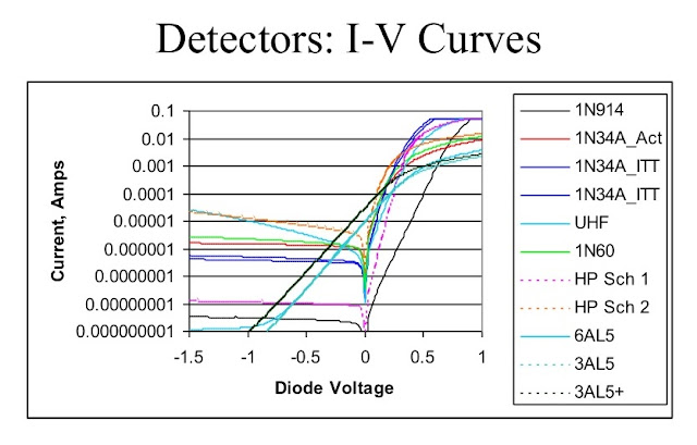
Choosing a diode for Z matching?


Expand the curves to see more clearly.

This is what they designed. Worth a try?

Thursday, April 19, 2018

Crystal Radio using Oat Mill Box

Oat Mill Box radio
The above link will download the magazine article with the construction details.
Here is the schematic for the more experienced builder. The article gives some info on the design.

Saturday, April 14, 2018

Making a chassis for a new amplifier.

*****Use caution when handling sheet metal. It will cut you. *****

When I was a kid an old can was a treasure. They made them a little thicker and did not crinkle them. The cans are not as suitable as they once were but we can still find some metal if we look. Flashing is a good material for a small chassis. A pizza or cookie pan provides a good sized piece of metal. I needed a little chassis for an amp and thought a couple of pictures could be in order. I made an amp a few days ago using a 2" X 4" junction box cover as the face plate. It was a good size so a 4" chassis should be fine. I cut a piece of flashing about 6" X 6". No I didn't measure it was the biggest piece I could get from a piece of scrap.
This is the sheet and the tools used. the scissors are 5" and the duck billed pliers are 6". The pliers are 1/4" wide smooth jawed. I used the hinge as a square to do my layout. Nothing special here. A very quick and dirty job. You could take time to do a good layout and get a better product.
I just came about 1" off each corner and made 4 cuts to define the top of the chassis.
I used the jaw width of my pliers as a guide and folded the flaps in on all four corners. This cut edge is not smooth but the folded edge is. no worry of being cut with it.
I folded the four sides and then bent them up. As you can see the edges are smoother than a cut edge would be. You can also see a ripple in my bend. I will smooth it after folding the corners in. If you look you can see the corners sticking up a little taller than the edge facing you. In order to lock the corners I will unfold the ends of the edge facing you and tuck the corner into it. Then when I crush the seam it will lock the corner in place.

The finished product. After folding the corners in and locking everything in place I "ironed" the edges to smooth it out. I now have a 3-3/4" X 4" X 5/8" chassis. I buy the pizza pans at Dollar Tree. When they get used a few times I get them for the scrap bin. They are thick enough to make a good chassis.

This is the amp I plan to put on the chassis.
AF Amp
The handy box plate has two mounting holes so all I need are a couple of angle brackets. I made some last week I think will work.

Thursday, April 12, 2018

Point of reference, Threshold, Knee???

Exploring the mystery of threshold. I know an old guy who will spit hit teeth out and go into a rage if you say a diode or transistor has a threshold. When I told him it was a generally accepted thing being taught in every school of electronics in the world. He said the schools were all wrong. So I begin the journey to unravel his adamant position. First "knee" is a term in common use in mathematics.
The knee of a curve is the point where its tangent has a slope of 1.  His answer is to use log graph and the knee goes away. Well! Yea this is why we us log paper to graph curves which follow a log function.
But what we were talking about was more like this. Forward bias for Germanium is 0.3V and for Silicon is 0.7V. Again he blows a gasket and says "NO,NO,NO there is no forward bias point. It is conducting below that point.".
Then he says it a piece wise function? No explanation of what that means to him. Because the curve is nonlinear it was difficult to build a model for it. The piece wise modeling scheme helps answer this problem. We still see a "Knee". In this case it is where the curves transitions between the linear and square law function.
Above Von the function is linear below it is square law.

Another problem with the modeling is its response to temperature.


Someone posted a bit of a Ben Tongue paper and I finally see the issue. You can go to bentongue.com and find a treasure trove of info on crystal set design. Mr Tongue says the threshold has no meaning in crystal set design. If you read his paper it may sound like having a small signal is a benefit. In detector design we have small signal and large signal detectors. I will post a couple of graphs showing their responses.

This is a large signal response. If the voltage is above threshold it is large and linear. In other words a large input produces a large output.
This is a small signal detector curve. At first glance they may appear the same. Look at the scale. The small signal is below threshold and so is the output. Note the log graph is "distorting" our view. Let's try another graph.

This graph being linear you can see the effect of the square law detector. So the analysis of a crystal set will show we see a gain in the detector circuit. Mr Tongue explains this and give some analysis of the impedance matching effects. Here is where the problem comes to light. The crystal set functions without any amplification other than what the circuit can provide. A high Q tank can boost the signal and the square law detector can boost the signal. If we had a signal strong enough to operate in the linear region it would be a good thing I don't think we would want to attenuate the signal to force square law detection. How can this be? When teaching introductory level classes we use something like this:

Using an ideal diode this is true and with large signal detection it is still close enough. But with small signal detection we are operating below the threshold and the detector is not switching it is acting as a non linear device. In other words rather than clip the negative half cycle it reduces its amplitude. The effect is rather than passing half the signal amplitude it is passing half plus a suppressed negative half cycle. So the filter capacitor charges to a voltage above half the input and the DC bias it produces is what the output rides on.
Take another look at the center signal and add negative pulses a quarter the amplitude of the positive pulses and shift the zero reference down.
If the input peaks at 8mv and we chop it to get 4mv with the ideal diode then add back 1mv because the diodes doesn't switch cleanly we get a 25% boost in signal.


Monday, April 9, 2018

stage gain? voltage gain, current gain, DB, DBM


The question is what is a stage gain and the answer is different from each reference. Can they all be correct? How can a gain of 0 equal a gain of 1 and equal a gain 8db? I guess the first step is to determine what gain we may be looking at. This link leads to a site with a calculator and some explanation of terms.
http://g4urh.co.uk/amateur_radio/calculating_dbm.php
The first thing you see there is this.
OK so 1mw at 600 ohms is 774.6mv. The only question here is why 1mw?
Now we see 1mw at 50 ohms =223.6mv. Again at 1mw why?

The standard is 0dbm which is 1 mw with a 600 ohm load. Or as stated above 774.6 mv drop across a 600 ohm load. If all our measurements were across a 600 ohm load it would be simple to use a meter and read dbm direct. When the load changes the game changes. Now let's look at the stage characteristics.

They say current gain is infinite! Assuming the input current was zero it would be. In the real world we have some current so we will look at that more later.
The voltage gain is very near 1. So we are told the current gain is limited by the load current at a voltage level close to the input. Now let's look at the circuit.
The chart states Zin = infinity. As you can see there is a couple of resistors in the circuit. You could do some math and figure all the resistors in parallel to find the Zin. I'm just going to use 300k which is a nice high value. We must assume an input voltage so I go with 1mv. Now back to the site linked above to see what db level 1mv at 300k would be.
So 1mv at 300k is -85dbm. Now assuming a voltage gain of 1 what would the output be in dbm with a 200 ohm load?
Remember our reference is 0dbm so we are down 53 dbm on the output and were down 85 dbm on the input. The reference quoted said the circuit had a gain of 0. That was that guys way of saying it gave no increase or had a unity gain. The voltage gain is 1. What is the power gain? 85-53=32 so our circuit has a gain of 32dbm ( the m references power gain). A voltage gain of 1 is a 0 db gain. Hey! maybe the guy in the reference meant 0dbv gain which is also correct?

What if the output was 50 ohm?
Now it is 47dbm with the 85dbm input we would have a gain of 38dbm.
So what have I learned from this exercise? Let's look at a circuit with dual output and see.

In this sample circuit I am using the JFET as an electronic transformer to match the load. My load can be either 60 ohm earbud or 2k ohm headset. What would the output be?
The sim shows a -62 dbm output to an earbud.
The sim shows a -51 dbm output to a 2k headphone.
I could optimize the circuit and make it more efficient for either purpose but it would drive either an earbud or headphone as is. (The sim is using -80dbm drive)
Hopefully that makes since and you can see the terms are relative and you need to know the point of reference to use the numbers.